Semiconductor wafer handling equipment is one of the most important equipment in the semiconductor industry's processing procedures. When transferring wafers, ceramic end effector are used to grab and clamp semiconductor wafers. Advanced ceramic materials are widely used in the manufacture of ceramic arms (also called handling arms) for the semiconductor field due to their excellent wear resistance, corrosion resistance, and low thermal expansion coefficient.
Ceramic End Effector in semiconductor equipment There are tens of millions of chip manufacturing processes, and the "handling process" is naturally indispensable. In the process of moving the wafer from process A to process B, how to repeatedly transport and process the wafer at high speed and cleanly has a huge impact on the quality of the finished wafer."High speed" and "cleanliness" are the core characteristics of semiconductor wafer handling equipment. To meet these characteristics, the equipment has extremely stringent performance requirements for the components used. Since most processes are carried out in a vacuum, high temperature, and corrosive gas environment, the handling arms used in the equipment must have excellent physical properties, such as: high mechanical strength, corrosion resistance, high temperature resistance, wear resistance, high hardness, and insulation. During the operation of semiconductor equipment, ceramic arms are required to transport wafers. Since the silicon wafers cannot be contaminated, this is generally carried out in a vacuum and clean environment. In a vacuum environment, most robotic arms made of other materials cannot meet the requirements. At this time, ceramic arms with high temperature resistance, wear resistance, and high hardness are needed to complete the task.
Advantages of ceramic end effector: 1)Ceramic end effector are more resistant to acid corrosion and alkali corrosion. They have a longer service life when processing semiconductors. 2)Ceramic end effector are not easy to react with other substances, and will not leave contaminated fine particles and charged charges on the contacted objects, will not generate metal ions, and will not contaminate semiconductor parts. 3) When the semiconductor is heat treated, the ceramic end effectoris less deformed by heat, reducing the deformation of semiconductor parts during heat treatment. 2. Materials of ceramic arms for semiconductor equipment People usually use high-purity alumina and silicon carbide to prepare ceramic arms. Both raw materials have physical properties such as high hardness, good wear resistance and high temperature resistance, and are excellent materials for preparing ceramic arms. (1) Alumina can be used to prepare most semiconductor ceramic parts. Depending on its content, the performance of the prepared products also varies. Alumina ceramic parts with a purity of 95% are white, and alumina ceramic products with a purity of 99% are ivory. It has excellent rigidity, strength, and durability, and is resistant to high temperatures, corrosion, and plasma erosion. (2) Silicon carbide ceramics are black in color, have high thermal conductivity, high strength, high hardness, are not easy to deform, have good shock resistance, and are also resistant to high temperatures and corrosion. Compared with alumina ceramics, they are light in weight.
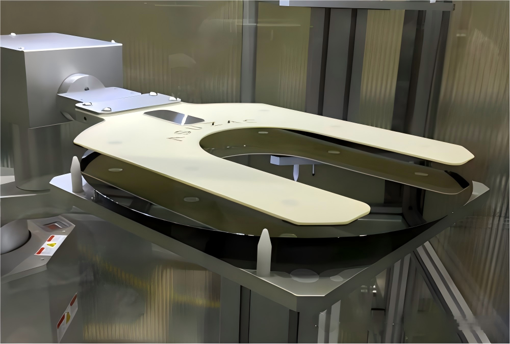
Ceramic robotic arms have high technical barriers. Ceramic robotic arms utilize the Bernoulli principle: gas introduced from the supply port is ejected at high speed from nozzles on the inner cylindrical side of the suction cup, forming a rotating airflow within the cylindrical space inside the suction cup and creating negative pressure. The airflow is ultimately released into the external space through the gap between the suction surface of the robotic finger and the wafer surface. The airflow forms a stable laminar flow in the space between the cyclonic suction cup and the wafer, creating a pressure difference between the upper and lower surfaces of the wafer, ultimately forming an upward suction force on the wafer.
There are air holes and ventilation grooves inside the ceramic arm. The grabbing and placing actions of the ceramic arm are generally achieved through vacuum adsorption and release. When the air is pumped out, a vacuum can be formed to adsorb the wafer. It must be fast and gentle, without impact and vibration. The suction device will not damage the wafer during the process of grabbing the sheet, and it must not introduce any pollution to the entire production operation room. There are currently two main methods for preparing ceramic arms: one is to first fine-process the ceramic plates, and then rely on the combination of ceramic plates to form an airway. The ceramic plates are usually fixed with an adhesive, but the adhesive will gradually age with the increase in use time and is difficult to use in harsh environments such as high temperature and corrosion, resulting in a short service life of the ceramic arm. The other is to introduce an inner model core to co-form the ceramic blank, and then remove the core by physical or chemical methods, and finally sinter to obtain a ceramic arm with a closed airway.


